Resources

Resources

Resource Center

  • AFM Lithography-Dynamic Plowing

    AFM Lithography-Dynamic Plowing

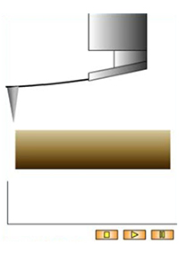
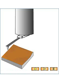
    AFM enables the direct machining the sample surface by means of AFM cantilever tips. This can be achieved in two ways, called Static Plowing (Scratching) and Dynamic Plowing. In the static plowing the AFM is employed in contact mode to pattern a sample surface or some layer on them, e.g. single resist layer and subsequently use it as an etch mask. This technique, while being a low-cost and low-effort technique, presents some drawbacks.

    It has been proved that, while cutting a furrow into the resist by static plowing, torsion of the cantilever may lead to edge irregularities. Additionally, depending on the local stiffness of the sample, while imaging the surface before or after the modification, further modifi- cations may occur due to dragging of the surface.

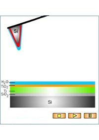
    By Dynamic Plowing Lithography (DPL) the surface is modified by indenting it with a vibrating tip in the AFM semicontact mode. This method provides a lithography technique that is nearly free from problems due to cantilever torsion and permits to image the modified surface without any further modification.

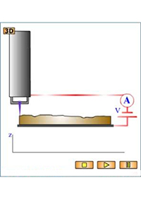
    Dynamic Plowing Lithography can be performed in a vector scan mode or in an image pattern scan mode. In the vector scan mode, the software provides a set of commands that permit us to write lines of arbitrary length and direction with defined scan speed and oscillation amplitude. The image pattern scan mode (see Example), is a synchronization of the raster scan mode with the desired pattern. The pattern can be constructed with a simple pixel-oriented paint program.

    The non-contact mode has the advantage that the tip never makes contact with the sample and therefore cannot disturb or destroy the sample. This is particularly important in biological applications.

    References

    1. J. Appl. Phys. 85, 3897 (1999).

    2. Rev. Sci. Instrum. 72, 136 (2001).


  • AFM Lithography-Scratching

    AFM Lithography-Scratching

    Ploughing is a well-known technique used since the earliest days of agricultural cultivation. By scaling this tool down in size to a few nanometers and combining it with conventional scanning probe techniques, one can facilitate nanolithography with nanometer resolution.

    In the more common AFM scratching techniques, the tip is scanned under strong loading forces to remove the substrate or resist. This technique utilizes the principle of ploughing in the same way as the traditional tool: material is removed from the substrate in a well-defined way, leaving behind deep trenches with the characteristic shape of the plough used.

    The advantages of applying a nanoscratching for lithography are obviously the precision of alignment, the nondamaging definition process compared to electron- or ion-beam structuring techniques, and the absence of additional processing steps, such as etching the substrate. Nanoploughing (nanoscratching) was applied, for example to defining supereconducting nanoconstrictions(Josephson junctions) [1], surface quantum wells patterning [2].

    When the AFM is operated in contact mode, not only deep scratching but also several regimes from frictionless sliding to permanent wear are observed, depending on the applied load. In this way, AFM has been successfully used to characterize microwear processes on materials of technological interest, as silicon for magnetic head sliders, polymers for electronic packaging and liquid crystals displays etc as is reviewed in [3].

    In NTMDT devices two different nanolithography modes are possible: vector and raster. In the case of vector lithography the influence is applied in single points or along the determined lines. In the case of raster lithography it is made from the already determined template. The advantage of vector lithography is a high speed while disadvantage is that the force is equal in each point. Raster lithography is slower, but it enables to change the force applied according with the template. Besides there are two ways to change the applied force when making vector lithography: 1. Changing of the beam bending by setting of the scanner displacement on defined distance along Z axis. 2. Changing of the beam bending, by setting of the SetPoint value. When doing raster lithography you can use only the first way.

    References

    1. Appl. Phys. Lett., Vol. 73, 2051 (1998).

    2. Appl. Phys. Lett., Vol. 73, 2684 (1998).

    3. Chem. Rev. 97, 1163 (1997).


  • AFM Oxidation Lithography

    AFM Oxidation Lithography

    AFM Anodic Oxidation Lithography is a kind of the AFM Voltage Lithography. With the help of the Voltage Lithography not only geometrical properties of the surface but also the local electrophysical properties of the sample surface can be changed. For example, by application of voltage to conductive cantilever the electrochemical processes on the surface can be stimulated under the probe tip and metalic layer can be oxidased.

    Particularly tip-induced oxidation of the surface of hyperfine titanium film on the silicon substrate under normal conditions is demonstrated on the animated picture [1]. In air or other humid atmosphere the probe and the surface of the sample are covered by thin film of absorbed water. When the tip approaches sufficiently close to the surface, these absorbed layers come in contact and water bridge is produced because of capillary effect. With application of a corresponding electric field the electrochemical reaction in water-surface border, in water and in the probe will be initiated through that bridge. If the surface is positively charged and the tip negatively, then the tip and the surface will interact electrochemically as anode and cathode correspondingly. Oxide will grow on the point right under the tip.

    For complex pictures Raster Lithography can be execute by using PCX-file [2]. Difference between minimum and maximum tone voltage will be applied proportionally to brightness and, correspondingly, anode oxide will grow to a different height forming different contrast of topographical image.

    References

    1. Nanotechnology 12, 273 (2001).

    2. "1st euspen topical conference on fabrication and metrology in nanotechnology". -Copenhagen, 2000. V.1, р.222-228.


  • STM Lithography

    STM Lithography

    An STM can modify the surface and material can be transported from the tip to the sample and back. If these actions can be performed in a controlled way widespread possibilities would arise: information storage devices, nanometer patterning technique, manipulations of big molecules and individual atoms, building of small devices.The most straightforward way to machine a surface by STM is by pushing the tip into the surface. This can result in a hole, but the tip can be damaged.

    More protective STM tip influence is use of the current pulse. The sample surface under the tip can be melted and evaporates.

    As Example of STM Lithography is presented STM image of three monolayers conducting LB film after local exposure to three electric pulses. Crater-like defects of one monolayer depth are readily seen.

    References

    1. Biosensor & Bioelectronics 11, 923 (1996).


  • ×

    13817907735