Resources

Resources

Resource Center

  • Contact mode

    Contact mode

    Contact mode is the basis for all AFM techniques in which the probe tip is in constant physical contact with the sample surface. While the tip scans along the surface, the sample topography induces a vertical deflection of the cantilever. A feedback loop maintains this deflection at a preset load force and uses the feedback response to generate a topographic image.


    Contact mode is suitable for materials science, biological applications and basic research. It also serves as a basis for further SPM techniques that require direct tip-sample contact.


  • Constant Force mode

    Constant Force mode

    In Contact mode of operation the cantilever deflection under scanning reflects repulsive force acting upon the tip.

    Repulsion force F acting upon the tip is related to the cantilever deflection value x under Hooke's law: F = -kx, where k is cantilever spring constant. The spring constant value for different cantilevers usually vary from 0.01 to several N/m.

    In our units the vertical cantilever deflection value is measured by means of the optical registration system and converted into electrical signal DFL. In contact mode the DFL signal is used as a parameter characterizing the interaction force between the tip and the surface. There is a linear relationship between the DFL value and the force. In Constant Force mode of operation the deflection of the cantilever is maintained by the feedback circuitry on the preset value. So vertical displacement of the scanner under scanning reflects topography of sample under investigation.

    Constant Force mode has some advantages and disadvantages.

    Main advantage of Constant Force mode is possibility to measure with high resolution simultaneously with topography some other characteristics - Friction Forces, Spreading Resistance etc.

    Constant Force mode has also some disadvantages. Speed of scanning is restricted by the response time of feedback system. When exploring soft samples (like polymers, biological samples, Langmuir-Blodgett films etc.) they can be destroyed by the scratching because the probe scanning tip is in direct contact with the surface. Thereunto under scanning soft unhomogeneous samples the local flexure of sample surface varies. As a result acquired topography of the sample can prove distorted. Possible existence of substantial capillary forces imposed by a liquid adsorption layer can decrease the resolution.

    References

    1. Magonov, Sergei N. Surface Analysis with STM and AFM. Experimental and Theotetical Aspects of Image Analysis.VCH 1996.


  • Constant Height mode

    Constant Height mode

    In Contact mode of operation the cantilever deflection under scanning reflects repulsive force acting upon the tip.

    Repulsion force F acting upon the tip is related to the cantilever deflection value x under Hooke's law: F = -kx, where k is cantilever spring constant. The spring constant value for different cantilevers usually vary from 0.01 to several N/m.

    In our units the vertical cantilever deflection value is measured by means of the optical registration system and converted into electrical signal DFL. In contact mode the DFL signal is used as a parameter characterizing the interaction force between the tip and the surface. There is a linear relationship between the DFL value and the force. In Constant Height mode of operation the scanner of the microscope maintains fixed end of cantilever on the constant height value. So deflection of the cantilever under scanning reflects topography of sample under investigation.

    Constant Height mode has some advantages and disadvantages.

    Main advantage of Constant Height mode is high scanning speeds. It is restricted only by resonant frequency of the cantilever.

    Constant Height mode has also some disadvantages. Samples must be sufficiently smooth. When exploring soft samples (like polymers, biological samples, Langmuir-Blodgett films etc.) they can be destroyed by the scratching because the probe scanning tip is in direct contact with the surface. Thereunto under scanning soft samples with relatively high relief the pressure upon the surface varies , simultaneously varies local flexure of sample surface. As a result acquired topography of the sample can prove distorted. Possible existence of substantial capillary forces imposed by a liquid adsorption layer can decrease the resolution.

    References

    1. Magonov, Sergei N. Surface Analysis with STM and AFM. Experimental and Theotetical Aspects of Image Analysis.VCH 1996.


  • Semicontact mode

    Semicontact mode
  • Lateral Force mode

    Lateral Force mode

    Lateral Force mode allows to distinguish areas with different friction and also to obtain edge-enhanced images of any surface. This capability may be used in conjunction with topographical images during one scan to characterize your samples more completely.

    The physical basics of the Lateral Force mode are as follows. When scanning in the Constant Force mode perpendicularly to longitudinal axis of the cantilever, besides the cantilever's deflection in the normal direction, an additional torsion bending of the cantilever occurs. It is caused by the moment of forces acting on the tip. With minor deflections, the angle of torsion is proportional to the side (lateral) force. The cantilever's torsion bending is measured by the microscope optical recording system.

    When moving over a flat surface with zones of different friction factors, the angle of torsion will be changing in every new zone. This allows measuring of the local friction force. If the surface is not absolutely flat, such an interpretation is complicated. To distinguish zones of different friction and relief influence one can utilize second pass on the same line in opposite direction. Nevertheless, this type of measuring allows obtaining images with clearly seen minor relief details and facilitates their search. In addition, the lateral force measuring mode easily provides the atomic resolution on mica and some other laminar materials.

    Lateral Force mode has important usage for semiconductors, polymers, deposited films, data storage devices, investigative studies of surface contamination, chemical speciation and frictional characteristics, and a growing list of new applications.

    References

    1. Phys. Rev. Lett. 59, 1942 (1987). 2. Magonov, Sergei N. Surface Analysis with STM and AFM. Experimental and Theotetical Aspects of Image Analysis. VCH 1996.


  • Force modulation mode

    Force modulation mode

    Under realization of Force Modulation mode (FM-mode) along with scanning of sample surface as in Constant Force mode (CFC-mode) the scanner (or the sample) executes a vertical periodic motion [1]. Under this periodic motion cantilever "feels out" the sample surface. At that the pressure of the probe tip on the sample surface does not remain constant but has periodic component, usually sinusoidal. In accordance with the local elasticity of the sample value of corresponding indentation will change under scanning. On the stiff areas of the sample surface depth of indentation will be smaller, and on the compliant areas - larger.

    Tracing of the sample surface relief height is conducted by the usage of the averaged cantilever deflection in the feedback circuit [2]. If values of the scanner vertical displacement Dz, the probe tip vertical displacement D and cantilever force constant кс are known, one can determine the local elasticity of the sample under investigation кs.

    кs = кс · (Dz/D - 1)

    In turn with known value of the local elasticity one can to determine the modulus of elasticity of the sample. It can be done with usage of the calibrating measurements or with usage of the Hertzian model [3]. Force Modulation mode is widely used in polymers, semiconductors, biological, especially in composite materials investigations.


    References

    1. US Pat. 5092163.

    2. Nanotechnology 2, 103 (1991).

    3. Jonson KL. Contact mechanics. Cambridge University press: Cambridge, 1995.


  • Phase_Imaging

    Phase_Imaging
  • Spreading Resistance Image

  • Elecric Force Microscopy

    Elecric Force Microscopy

    Fig. 1. A set-up for AFM-based electrostatic modes and possible configurations of lock-in amplifiers for multi-frequency electrostatic force studies.

    The AFM modes, which are based on the detection of tip-sample electrostatic forces [1], include Electrostatic force microscopy (EFM), Kelvin probe force microscopy (KPFM) and probing of local dielectric properties in various configurations including Maxwell stress microscopy and others [2], [3]. These modes were introduced for mapping the variations of electrostatic force, measurements of local surface potential and dielectric permittivity.

    In these methods a conducting probe exercises the electrostatic force of a sample, which can be rationally modeled by considering a probe tip as an electrode in a tiny capacitor which it forms with the sample that acts as the second electrode, Figure 1 (right). For the operation of AFM-related electrostatic modes the probe is driven into a mechanical oscillation by a piezo-shaker at its flexural mode, ωmech, and the electrostatic forces are stimulated by a DC electric bias applied to the probe and/or an AC bias either at ωmech or at other frequency, ωelec. While scanning, the conducting probe simultaneously senses the mechanical and electrostatic force interactions with the sample.

    The effects of these interactions can be decoupled either by performing these measurements in separate passes at the same frequency (two-pass technique) or in the single-pass with the simultaneous detection of the mechanical and electrostatic interactions at different frequencies [2]. The latter approach requires a use of several lock-in amplifiers in the detection system, Figure 1 (left).

    References

    1. Y. Martin, D. A. Abraham, and H. K. Wickramasinghe “High-resolution capacitance measurement and potentiometry by force microscopy” Appl. Phys. Lett. 1988, 52, 1103–10005.

    2. S. Magonov, J. Alexander, and S. Wu “Advancing characterization of materials with Atomic Force Microscopy – based electric techniques”. In Scanning Probe Microscopy of Functional Materials: Nanoscale Imaging and Spectroscopy; Kalinin, S. V.; Gruverman, A., Eds.; Springer: Berlin, Germany, 2010; pp 233–300.

    3. H. Yokoyama, and M. J. Jeffery “Imaging high-frequency dielectric dispersion of surfaces and thin films by heterodyne force-detected scanning Maxwell stress microscopy” Colloids Surf. A 1994, 93, 359–373.


  • Magnetic Force Microscopy

    Magnetic Force Microscopy

    Magnetic Force microscopy (MFM) [1,2] is an effective tool for magnetic investigations on submicron scale. Image obtained by MFM is the space distribution of some parameter characterizing magnetic probe-sample interaction, i.e. interaction force, amplitude of vibrating magnetic probe etc. The magnetic probe is standard silicon cantilever (or silicon nitride cantilever) coated by magnetic thin film. MFM measurements enable the high resolution investigation of magnetic domain structure, reading and recording information in magnetic media, magnetization reversal processes etc.


    In magnetic investigations on submicron scale first of all one must separate the magnetic image from the topography. To solve this problem the magnetic measurements are executed by means of two-pass method. In the first pass the topography is determined in Contact or Semicontact mode. In the second pass the cantilever is lifted to a selected height for each scan line (or after topography measurement), and scanned using the stored topography (without the feedback). As a result the tip-sample separation during second pass is kept constant. This tip-sample separation must be large enough to eliminate the Van der Waals’ force. During second pass the short-range Van der Waals’ force vanishes and the cantilever is affected by long-range magnetic force. Both the height-image and the magnetic image are obtained simultaneously with this method.


    In the DC MFM during second pass the deflection (DFL) of a non-vibrating cantilever is detected. DFL is caused by the magnetic interaction between the tip and the sample (similarly to contact mode). The magnetic force acting on the cantilever can be obtained by multiplying the deflection of the cantilever by the cantilever force constant. Due to a small size of the magnetic cantilever it is possible to consider it as a point magnetic dipole. In this approximation the force F acting on the cantilever during the second pass can be written in the form:


    F = (m grad) H


    where m is the effective magnetic moment of the cantilever, H is the stray field from the sample. This equation is the Zeeman energy derivative taken with the inverse sign.


    References

    Appl. Phys. Lett. 50, 1455 (1987).


    J. Appl. Phys. 62, 4293 (1987).


  • Scanning Kelvin Probe Microscopy

    Scanning Kelvin Probe Microscopy

    Kelvin probe force microscopy (Kelvin mode of Scanning Probe Microscopy) was invented for measuring contact potential difference between the probe and the sample [1]. At present time Kelvin mode is based on the two-pass technique. In the first pass the topography is acquired using standard Semicontact mode (mechanical excitation of the cantilever). In the second pass this topography is retraced at a set lift height from the sample surface to detect the electric surface potential Ф(x). During this second pass the cantilever is no longer excited mechanically but electrically by applying to the tip the voltage Vtip containing dc and ac components

    Vtip = Vdc + Vac sin(wt)

    The resulting capacitive force Fcap between the tip and a surface at potential Vs is

    Fcap =(1/2) (Vtip - Ф(x))2(dC/dz)

    where C(z) is the tip-surface capacitance. The first harmonic force

    Fcap w = (dC/dz (Vdc - Ф(x)Vac)sin(wt)

    leads to suitable cantilever oscillations. The feedback then changes the dc tip potential Vdc until the w component of the cantilever (and accordingly w component of the tip-force) vanishes, e.g. Vdc(x) became equal to Ф(x). So mapping Vdc(x) reflects distribution of the surface potential along the sample surface. If no special tip-sample bias voltage is applied this distribution is Contact Potential Difference distribution.

    References

    1. Appl. Phys. Lett. 58, 2921 (1991).


  • Scanning Capacitance Microscopy

    Scanning Capacitance Microscopy

    Scanning Capacitance Microscopy is kind of dynamic EFM. Generally [1] in EFM. the cantilever is biased directly by Vtip=Vdc + Vac sin(wt), where Vac is referred to as the driving voltage. Scanning is executed on some height h above the sample surface in according with the profile defined during the first scanning in Semicontact mode. The capacitive force Fcap(z) between the tip and a sample surface at potential Vs is

    Fcap(z) =(1/2) (Vtip - Vs)2(dC/dz)

    where C(z) is the tip-surface capacitance dependent on tip geometry, surface topography and tip-surface separation z.

    Second harmonic of the capacitive force depends only on (dC/dz) and Vac

    Fcap2w(z) =(1/2) (dC/dz)Vac2 sin(2wt)

    and can be used for acquisition additional information, e.g distribution of the surface capacity over the sample. For maximization of the second harmonic oscillations the ac frequency w is adjusted to be equal to half of cantilever resonance frequency wr.

    References

    1. Nanotechnology 12, 485 (2001).

    2. Appl. Phys. Lett. 52, 1103 (1988).

    3. J. Appl. Phys. 61, 4723 (1987).


  • Piezoresponse Force Microscopy

    Piezoresponse Force Microscopy

    The basic idea of Piezoresponse Force Microscopy (PFM) is to effect locally the piezoelectric sample surface by the electric field and to analyse resulting displacements of the sample surface[1].

    The PFM technique is based on the converse piezoelectric effect, which is a linear coupling between the electrical and mechanical properties of a material. Since all ferroelectrics exhibit piezoelectricity, an electric field applied to a ferroelectric sample results in changes of its dimensions.

    To detect the polarization orientation the AFM tip is used as a top electrode, which is moved over the sample surface.

    In the Intro 1 animation one can see the reaction of out-of-plane and in-plane domains in the ferroelectric film on the voltage applied to the scanning tip in Contact Constant Force mode. The electric field generated in the sample causes the domains with the polarization parallel to the field to extend and the domains with opposite polarization to contract.

    If the polarization vector is perpendicular to the electric field, there is no piezoelectric deformation along the field direction, but a shear strain appears in the ferroelectric, leading to displacements of the sample surface parallel to itself, along the polarization direction.

    The AFM probe tip moving according to the surface displacement causes cantilever normal or torsion (because of friction) deflections. Direction of the deflection depends on the mutual orientations of the electric field and domain polarization. Correspondingly in the case of the AC electric field (see Intro 2 animation) phase lag between the electric field and cantilever deflections will depend on the their mutual orientations. In general case by analyzing the amplitudes and phases of the normal and torsion cantilever vibrations one can reconstruct the sample domain structure.

    References

    1. M. Alexe, A. Gruverman (Eds.). Nanoscale Characterisation of Ferroelectric Materials. Scanning Probe Microscopy Approach. Springer, 2004.


  • Non-contact_mode

    Non-contact_mode

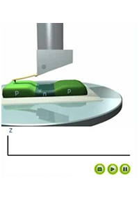
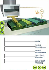
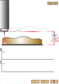
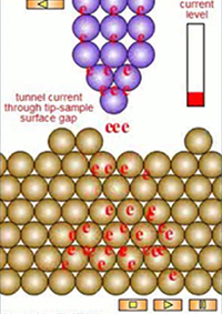
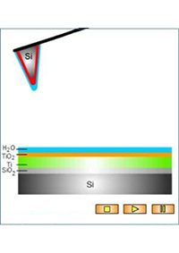
    The Non-Contact AFM (NC AFM), invented in 1987 [1], offers unique advantages over other contemporary scanning probe techniques such as contact AFM and STM. The absence of repulsive forces (presenting in Contact AFM) in NC AFM permits it use in the imaging “soft” samples and, unlike the STM, the NC AFM does not require conducting samples.

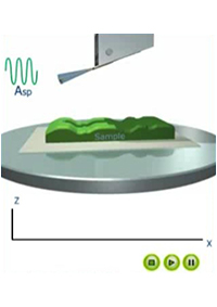
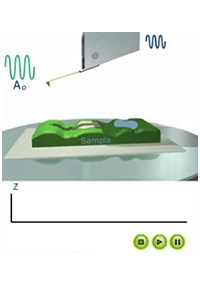
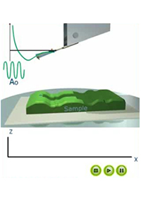
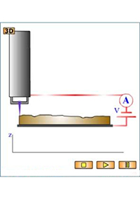
    The NC AFM works via the principle “amplitude modulation” detection. The corresponding detection scheme exploits the change in the amplitude, A, of the oscillation of a cantilever due to the interaction of a tip with a sample. To the first order, the working of the NC AFM can be understood in terms of a force-gradient model [1]. According to this model, in the limit of small A, a cantilever approaching a sample undergoes a shift, df, in its natural frequency, fo, towards a new value given by

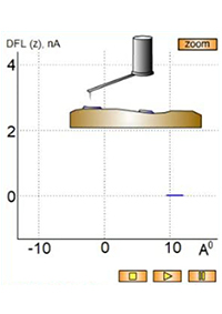
    feff = fo (1-F’(z)/ko )1/2

    where feff is the new, effective resonance frequency of the cantilever of nominal stiffness ko in the presence of a force gradient F’(z) due to the sample. The quantity z represents an effective tip-sample separation while
    df = feff - fo is typically negative, for the case of attractive forces.

    If cantilever is initially forced to vibrate at a fset > fo, then the shift in the resonance spectrum of the cantilever towards lower frequencies will cause a decrease in the oscillation amplitude at fset as the tip approaches the sample [1].

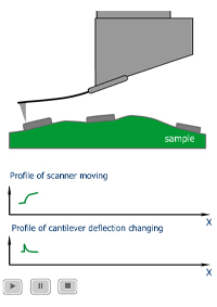
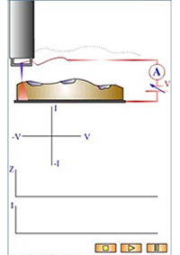
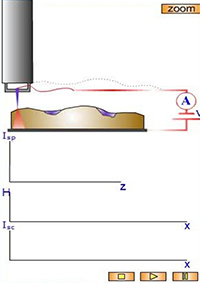
    This change in A is used as the input to the NC-AFM feedback. To obtain a NC AFM image the user initially chooses a value Aset as the set-point such that Aset < A(fset) when the cantilever is far away from the sample.

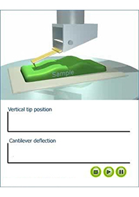
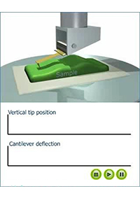
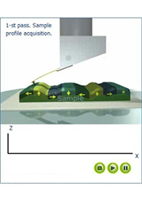
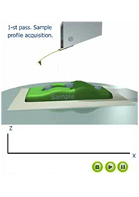
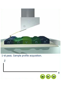
    The NC AFM feedback then moves the cantilever closer to the sample until its instantaneous oscillation amplitude, A, drops to Aset at the user-defined driving frequency fset. At this point the sample can be scanned in the x–y plane with the feedback keeping A = Aset = constant in order to obtain a NC AFM image. The NC AFM feedback brings the cantilever closer (on average) to the sample if Aset is decreased at any point, and moves the cantilever farther away from the sample (on average) if Aset is increased. Overall, the implication of the above model is that the NC AFM image may be considered, in the limit of small A, to be a map of constant interaction-force gradient experienced by the tip due to the sample.

    The non-contact mode has the advantage that the tip never makes contact with the sample and therefore cannot disturb or destroy the sample. This is particularly important in biological applications.

    References

    1. J. Appl. Phys. 61, 4723 (1987).


  • Constant Current mode

    Constant Current mode

    In STM bias voltage is applied between a sharp conductive tip and a conductive sample, so when the sample is approached to a few angstroms from the tip, tunneling current occurs, that indicates proximity of the tip to the sample with very high accuracy. In Constant Current mode (CCM) of operation when scanning sample surface the scanner keeps the current constant by feedback circuit. So vertical displacement of the scanner (feedback signal) reflects surface topography.

    STM gives true atomic resolution on some samples even at ambient conditions. Scanning tunneling microscopy can be applied to study conductive surfaces or thin nonconductive films and small objects deposited on conductive substrates. The speed of scanning in CCM is restricted by usage of feedback system. Larger scanning speeds can be obtained by usage of 
    Constant Height mode (CHM), but CCM allows to investigate the samples with developed relief.

    The tunnel currents registered in the course of the measurement are sufficiently small - up to 0.03 nA (with a special STM head - up to 0.01 nA), so it is possible to investigate also low conductivity surfaces, in particular biological objects.

    Among the STM disadvantages one can mention the complexity of the results interpretation for some surfaces since the surface image received in the STM investigation mode is determined not only by the surface relief but also by the density of states, bias voltage sign and value, current value etc. For example on the highly oriented pyrolitic graphite surface one can see only each second atom. It is concerned with special arrangement of wave functions density of states.

    References

    1. Rep. Prog. Phys. 55, 1165-1240 (1992).


  • Constant Height mode

    Constant Height mode

    In STM bias voltage is applied between a sharp conductive tip and a conductive sample, so when the sample is approached to a few angstroms from the tip, tunneling current occurs, that indicates proximity of the tip to the sample with very high accuracy. In Constant Height mode (CHM) of operation the scanner of STM moves the tip only in plane, so that current between the tip and the sample surface visualizes the sample relief. Because in this mode the adjusting of the surface height is not needed a higher scan speed can be obtained. CHM can only be applied if the sample surface is very flat, because surface corrugations higher than 5-10 A will cause the tip to crash. The weak feedback is still present to maintain a constant average tip-sample distance. As the information on the surface structure is obtained via the current, a direct gauging of height differences is no longer possible.

    STM gives true atomic resolution on the some samples even at ambient conditions. Scanning tunneling microscopy can be applied to study conductive surfaces or thin nonconductive films and small objects deposited on conductive substrates.

    The tunnel currents registered in the course of the measurement are sufficiently small - up to 0.03 nA (with a special STM head - up to 0.01 nA), so it is possible to investigate also low conductivity surfaces, in particular biological objects.

    Among the STM disadvantages one can mention the complexity of the results interpretation for some surfaces since the surface image received in the STM investigation mode is determined not only by the surface relief but also by density of states, bias voltage sign and value, current value etc. For example on the highly oriented pyrolitic graphite surface one can see only each second atom. It is concerned with special arrangement of wave functions density of states.

    References

    1. Rep. Prog. Phys. 55, 1165-1240 (1992).


  • I(V) Spectroscopy

    I(V) Spectroscopy

    In I(V) Spectroscopy (or Current Imaging Tunneling Spectroscopy, CITS) a normal topographic image is acquired at fixed Io and Vo. At each point in the image feedback loop is interrupted and the bias voltage is set to a series of voltages Vi and the tunneling current Ii is recorded. The voltage is then returned to Vo and the feedback loop is turned back on. Each I-V spectra can be acquired in a few milliseconds so there is no appreciable drift in the tip position. This procedure generates a complete current image Ii(x,y) at each voltage Vi in addition to the topographic image z(x,y)|VoIo.

    CITS data can be used to calculate a current difference image DIViVj(x,y) where Vi and Vj bracket a particular surface state, producing an atomic resolved, real space image of a surface state. This technique, for example can be used in UHV to image filled ad-atom states or the dangling bond states for silicon reconstructions.

    References

    1. G. Binnig and H. Rohrer: Surf. Sci. 126 (1983) 236. Rep. Prog. Phys. 55, 1165-1240 (1992).


  • I(z) Spectroscopy

    I(z) Spectroscopy

    The I(z) Spectroscopy is related to LBH spectroscopy and can be used for providing an information about the z-dependence of the microscopic work function of the surface. Next important use of the I(z) Spectroscopy is concerned with for testing of the STM tip quality.

    The tunneling current IT in STM exponentially decays with the tip-sample separation z as

    IT ~ exp(-2kz),

    where the decay constant is given by

    2k = 2(2mU/h2)1/2.

    U is the average work function Uav = (Us + Ut)/2, where Ut and Us are the tip and sample work functions, respectively.

    In the I(z) Spectroscopy, we measure the tunnel current versus tip-sample separation at each pixel of an STM image. For Uav = 1 eV, 2k = 1.025 A-1eV-1. Sharp I(z) dependence helps in determining of tip quality. As is empirically established if tunnel current UT drop to one-half with Z < 3 A the tip is considered to be very good, if with Z < 10 A, then using this tip it is possible to have an atomic resolution on HOPG.
    If this takes place with Z > 20 A this tip should not be used and must be replaced.

    References

    1. G. Binnig and H. Rohrer: Surf. Sci. 126 (1983) 236. Rep. Prog. Phys. 55, 1165-1240 (1992).


  • AFM Lithography-Dynamic Plowing

    AFM Lithography-Dynamic Plowing

    AFM enables the direct machining the sample surface by means of AFM cantilever tips. This can be achieved in two ways, called Static Plowing (Scratching) and Dynamic Plowing. In the static plowing the AFM is employed in contact mode to pattern a sample surface or some layer on them, e.g. single resist layer and subsequently use it as an etch mask. This technique, while being a low-cost and low-effort technique, presents some drawbacks.

    It has been proved that, while cutting a furrow into the resist by static plowing, torsion of the cantilever may lead to edge irregularities. Additionally, depending on the local stiffness of the sample, while imaging the surface before or after the modification, further modifi- cations may occur due to dragging of the surface.

    By Dynamic Plowing Lithography (DPL) the surface is modified by indenting it with a vibrating tip in the AFM semicontact mode. This method provides a lithography technique that is nearly free from problems due to cantilever torsion and permits to image the modified surface without any further modification.

    Dynamic Plowing Lithography can be performed in a vector scan mode or in an image pattern scan mode. In the vector scan mode, the software provides a set of commands that permit us to write lines of arbitrary length and direction with defined scan speed and oscillation amplitude. The image pattern scan mode (see Example), is a synchronization of the raster scan mode with the desired pattern. The pattern can be constructed with a simple pixel-oriented paint program.

    The non-contact mode has the advantage that the tip never makes contact with the sample and therefore cannot disturb or destroy the sample. This is particularly important in biological applications.

    References

    1. J. Appl. Phys. 85, 3897 (1999).

    2. Rev. Sci. Instrum. 72, 136 (2001).


  • AFM Lithography-Scratching

    AFM Lithography-Scratching

    Ploughing is a well-known technique used since the earliest days of agricultural cultivation. By scaling this tool down in size to a few nanometers and combining it with conventional scanning probe techniques, one can facilitate nanolithography with nanometer resolution.

    In the more common AFM scratching techniques, the tip is scanned under strong loading forces to remove the substrate or resist. This technique utilizes the principle of ploughing in the same way as the traditional tool: material is removed from the substrate in a well-defined way, leaving behind deep trenches with the characteristic shape of the plough used.

    The advantages of applying a nanoscratching for lithography are obviously the precision of alignment, the nondamaging definition process compared to electron- or ion-beam structuring techniques, and the absence of additional processing steps, such as etching the substrate. Nanoploughing (nanoscratching) was applied, for example to defining supereconducting nanoconstrictions(Josephson junctions) [1], surface quantum wells patterning [2].

    When the AFM is operated in contact mode, not only deep scratching but also several regimes from frictionless sliding to permanent wear are observed, depending on the applied load. In this way, AFM has been successfully used to characterize microwear processes on materials of technological interest, as silicon for magnetic head sliders, polymers for electronic packaging and liquid crystals displays etc as is reviewed in [3].

    In NTMDT devices two different nanolithography modes are possible: vector and raster. In the case of vector lithography the influence is applied in single points or along the determined lines. In the case of raster lithography it is made from the already determined template. The advantage of vector lithography is a high speed while disadvantage is that the force is equal in each point. Raster lithography is slower, but it enables to change the force applied according with the template. Besides there are two ways to change the applied force when making vector lithography: 1. Changing of the beam bending by setting of the scanner displacement on defined distance along Z axis. 2. Changing of the beam bending, by setting of the SetPoint value. When doing raster lithography you can use only the first way.

    References

    1. Appl. Phys. Lett., Vol. 73, 2051 (1998).

    2. Appl. Phys. Lett., Vol. 73, 2684 (1998).

    3. Chem. Rev. 97, 1163 (1997).


  • AFM Oxidation Lithography

    AFM Oxidation Lithography

    AFM Anodic Oxidation Lithography is a kind of the AFM Voltage Lithography. With the help of the Voltage Lithography not only geometrical properties of the surface but also the local electrophysical properties of the sample surface can be changed. For example, by application of voltage to conductive cantilever the electrochemical processes on the surface can be stimulated under the probe tip and metalic layer can be oxidased.

    Particularly tip-induced oxidation of the surface of hyperfine titanium film on the silicon substrate under normal conditions is demonstrated on the animated picture [1]. In air or other humid atmosphere the probe and the surface of the sample are covered by thin film of absorbed water. When the tip approaches sufficiently close to the surface, these absorbed layers come in contact and water bridge is produced because of capillary effect. With application of a corresponding electric field the electrochemical reaction in water-surface border, in water and in the probe will be initiated through that bridge. If the surface is positively charged and the tip negatively, then the tip and the surface will interact electrochemically as anode and cathode correspondingly. Oxide will grow on the point right under the tip.

    For complex pictures Raster Lithography can be execute by using PCX-file [2]. Difference between minimum and maximum tone voltage will be applied proportionally to brightness and, correspondingly, anode oxide will grow to a different height forming different contrast of topographical image.

    References

    1. Nanotechnology 12, 273 (2001).

    2. "1st euspen topical conference on fabrication and metrology in nanotechnology". -Copenhagen, 2000. V.1, р.222-228.


  • STM Lithography

    STM Lithography

    An STM can modify the surface and material can be transported from the tip to the sample and back. If these actions can be performed in a controlled way widespread possibilities would arise: information storage devices, nanometer patterning technique, manipulations of big molecules and individual atoms, building of small devices.The most straightforward way to machine a surface by STM is by pushing the tip into the surface. This can result in a hole, but the tip can be damaged.

    More protective STM tip influence is use of the current pulse. The sample surface under the tip can be melted and evaporates.

    As Example of STM Lithography is presented STM image of three monolayers conducting LB film after local exposure to three electric pulses. Crater-like defects of one monolayer depth are readily seen.

    References

    1. Biosensor & Bioelectronics 11, 923 (1996).


  • Force-distance curves

    Force-distance curves

    Force is measured in an SFM by collecting a force curve, which is a plot of cantilever deflection, dc, as a function of sample position along the z-axis (i.e. towards or away from the probe tip; the z-piezo position). It assumes a simple relationship (i.e. Hooke’s F = - k dc

    where k is the spring constant of the cantilever. Some other forces included in tip-sample interaction under dc approach or retracting motion are presented on the figure left [1]. Used definitions see below. The interpretation of AFM force curves relies almost entirely on established force laws, particularly those determined using the SFA [2]. These force laws describe force as a function of the probe–sample separation distance (D) rather than as a function of the z-piezo position. Thus, to be useful, the force curves must be transformed into descriptions of force as a function of distance, F(D). However, current SFMs do not have an independent measure of D. Instead, the transformation to D is achieved by subtracting the cantilever deflection from the z-piezo movement.

    For a very hard surface, zero separation is defined as the region in the force curve in which the cantilever deflection is coupled 1:1 with the sample movement; this appears in the force curve as a straight line of unit slope. A corrected curve is called a force–distance curve. Notice that determining D by this approach requires that the tip make contact with the sample. In practice, there are two factors (long-range forces and sample elasticity) that can make determining the point of contact very difficult. A complete force curve includes the forces measured as the probe approaches the sample and is retracted to its starting position. Because the forces on the tip can vary as it is moved toward or away from the sample, for the purposes of presentation, we will divide the force curve into approach and retraction portions and consider them separately.

    References

    1. TIBTECH 17, 143 (1999).

    2. Israelashvili, J.N. (1992) Intermolecular and Surface Forces, Academic Press.


  • Adhesion Force Microscopy

    Adhesion Force Microscopy

    The retracting portion of the force curve sometimes follows the approach curve; however, there is often hysteresis. The most common type of hysteresis is due to some sort of adhesion, which appears in the force curve as a deflection below the zero-deflection line. The source of the adhesion can vary depending on the sample. In the ideal case of a sphere interacting with a flat surface, the adhesion force can be related to the radius of the sphere and the surface energies of the two surfaces.

    Under ambient conditions, the main source of adhesion is the formation of a capillary bridge between the tip and the sample. In air, most samples have several nanometers of water adsorbed to the surface; this water layer wicks up the tip and forms a ‘bridge’ between the tip and the sample. Pulling the tip out of that bridge requires a large force to overcome the surface tension. In fluid, the adhesive force depends on the interfacial energies between the tip and sample surfaces, and the solution; varying the solution can thus change the force of adhesion.

    A different form of ‘adhesion’ occurs when a polymer is captured between the AFM tip and the substrate. In this case, there is a very distinctive ‘adhesive’ force as the tip is pulled away. Typically, these curves initially retrace the approach curve near the surface but, away from the surface, exhibit a smooth negative deflection as the polymer is stretched until it breaks or detaches from the tip or the substrate, and the cantilever returns to the zero-deflection line. If multiple polymer molecules attach to the tip and substrate, a saw-tooth pattern can be observed as individual polymers detach. For references concerning different kinds of adhesive forces see [1, 2].

    To be useful, the force curves must be transformed into descriptions of force as a function of distance, F(D). However, current SFMs do not have an independent measure of D. Instead, the transformation to D is achieved by subtracting the cantilever deflection from the z-piezo movement.

    In some cases detachment of the tip under retractive motion of scanner occurs abrupt, and suitable force (force of adhesion) can measured relatively correctly.

    Corresponding adhesion maps are typically produced by taking the most negative force detected during the retraction curve as the value for adhesion and plotting that value against the x–y position of each curve. Several types of spatially resolved adhesion map can be produced, for example, the spatial distribution of adhesion in grafted-polymer systems. Using a special AFM tips, modified by antibodies or ligands, one can map the distribution of specific proteins on the surfaces of living cells etc.

    References

    1. TIBTECH 17, 143 (1999).

    2. Israelashvili, J.N. (1992) Intermolecular and Surface Forces, Academic Press.


  • Amplitude-distance curves

    Amplitude-distance curves

    Amplitude-modulation (intermittent-contact, semicontact) mode is widely spreaded oscillating mode and generally speaking can be interpreted and described by the amplitude, phase, frequency and dissipation on one another or on the cantilever-sample distance dependences.

    The study of such dependences is necessary according to following circumstances. First of all it relates to obtaining high-grade images (without noise and with high resolution). Then the study of suitable dependences can help in determining the nature of tip-sample interaction, defining forces included in this interaction and formation SPM images. At last the study of suitable curves can help in obtaining more contrastive images and quantitative parameters of sample under investigation.

    Obtained in Amplitude-modulation mode images are determined by the row of factors related to the sample as well as to conditions of measurement and values of scanning parameters.

    For interpreting results of amplitude-modulation mode usage one can to study dependence of oscillation amplitude the tip-sample distance. Suitable amplitude-distance (a-d) curves (their typical view one can see on the animated picture) can be monotonic or can to have areas of bistability and hysteresis. The presence of the bistability (as is shown on the same picture) leads to arising of the artifacts on the images obtained in Amplitude-modulation mode.

    Origin of bistability lies in possibility of simultaneously co-existence oscillations predominantly in attractive or predominantly in repulsive potentials.
    The bistability also can arise in complicated shape of tip-sample potential when in initial area cantilever stiffness is greater than potential derivative and the potential derivative becames greater tha cantilever stiffness.

    With suitable choise of set-point amplitude of cantilever oscillation, its stiffness, sharpness of the tip one can reach conditions when over all sample surface under investigation areas with bistability are absent.

    References

    1. Phys. Rev. B 60, 4961 (1999).

    2. Surface Sciece 460, 292 (2000).

    3. Phys. Rev. B 66, 041406 (2002).


  • ×
    共35条 每页25条 页次:1/2
    12Next last

    13817907735